BLOG
AI-Powered Visual Inspection in Electronics: PCB, Solder and Component Control
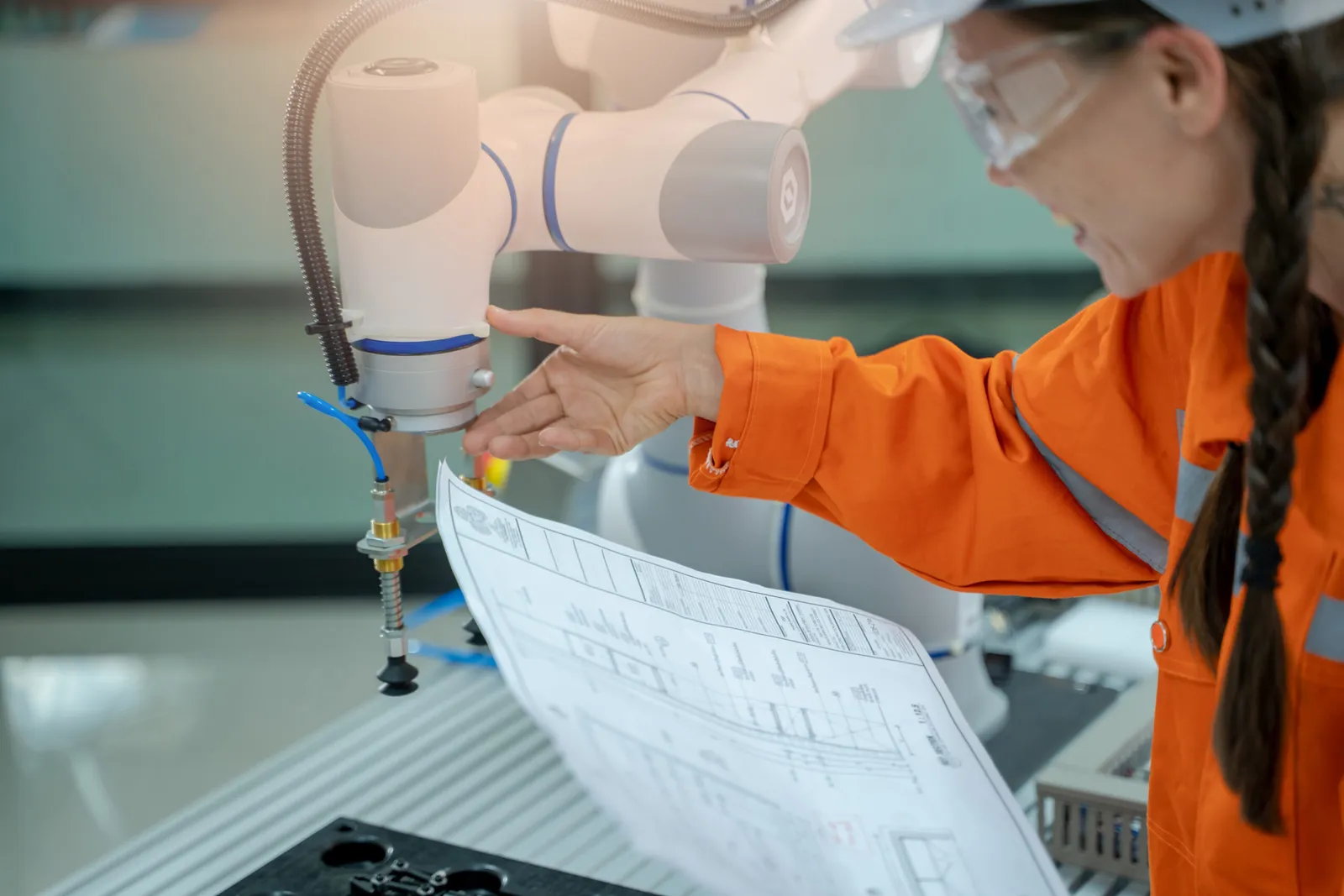
In Electronics, the Cost of a Defect Grows Exponentially
In electronics manufacturing, the later a defect is caught, the higher its cost. A missing component on a PCB, a shifted placement, a solder bridge or a cold joint turns into recalls, warranty claims and reputational loss when found in the field. With human visual inspection, miniature components, high-speed lines and operator fatigue make consistency hard to maintain.
AI-Powered Visual Inspection
MIS-INSPECT® makes visual quality control in electronics consistent with artificial intelligence and deep learning. The system evaluates criteria such as component presence and correct placement, solder quality, polarity, and label and print accuracy at high speed. In cases with high surface and lighting variability where classic rule-based methods struggle, deep learning provides stability in defect classification.
Deep Learning with Solomon and Zebra Aurora
MIS Automation integrates Solomon and Zebra Aurora technologies as the deep-learning software foundation in its visual inspection solutions. This approach catches low-contrast defects on variable surfaces with models that learn from many samples, eliminating the burden of reprogramming rule-based systems for every variation.
Which Applications?
- Component presence/absence and placement checks on PCBs
- Solder quality, bridge and missing-solder detection
- Connector, pin and polarity verification
- Label, print and data-matrix readability checks
- Surface scratch, dent and cosmetic-defect detection
The Difference Between Classic AOI and Deep Learning
Classic AOI (Automated Optical Inspection) systems are rule-based: thresholds and templates are defined for each defect type and variation. This approach creates a reprogramming burden as product variety and surface variability grow, and can increase false positives on low-contrast defects. Deep-learning-based inspection, by contrast, learns from many samples and gives more stable defect classification under variable surface, shadow and print conditions.
It is important to remember that the result depends not only on software but also on lighting and optics. Lighting placed at the right angle manages challenges such as solder glare or surface reflection, while suitable lenses and resolution allow miniature components to be distinguished. MIS-INSPECT® addresses lighting, optics, model training and line integration together to build stable inspection in the field.
Frequently Asked Questions
Do I have to fully replace my existing AOI system?
No. Depending on the application, a deep-learning layer can be positioned as a complement for defect types (low-contrast, variable) where classic AOI struggles.
I have few defective samples; can a model be trained?
Modern approaches include methods that work with limited defective samples; classification stability improves as data grows. A data strategy is planned at the start of the project.
Which defect types does it catch?
Component presence/absence and placement, solder bridges and missing solder, polarity, label/print readability and surface cosmetic defects are the main applications.
Can it keep up with my production speed?
The solution is designed by selecting the camera, optics and processing architecture according to the line’s cycle time; the goal is consistent inspection without slowing the line.
Done Right, Quality Control Creates Value
AI-powered quality control is not just adding a camera; it is designing the right lighting, optics, model training and line integration together. Done right, MIS-INSPECT® reduces escaped defects while lowering rework and scrap costs and making production data traceable. Contact the MIS Automation team for a visual inspection scenario suited to your electronics line.